 English
 Español
 Português
 русский
 Français
 日本語
日本語 Deutsch
 tiếng Việt
 Italiano
 Nederlands
 ภาษาไทย
 Polski
 한국어
한국어 Svenska
 magyar
 Malay
Malay বাংলা ভাষার
 Dansk
Dansk Suomi
Suomi हिन्दी
 and low temperature polysilicon (LTPS) for project development with display - News - SZ Hongjia Technology Shares Limited")

How to choose between amorphous silicon (a-Si) and low temperature polysilicon (LTPS) for project development with display
1. Introduction to LTPS
Low Temperature Poly-silicon (Low Temperature Poly-silicon; LTPS, hereinafter referred to as LTPS) is another new technology in the field of flat panel displays. Next-generation technology following amorphous silicon (Amorphous-Silicon, hereinafter referred to as a-Si).
Polysilicon (polysilicon) is a silicon-based material with a size of about 0.1 to several um, which is composed of many silicon particles. In the semiconductor manufacturing industry, polysilicon is usually treated by LPCVD (Low Pressure Chemical Vapor Deposition), and then annealed at a temperature higher than 900C. This method is called SPC (Solid Phase Crystallization). However, this method is not suitable for the flat panel display manufacturing industry, because the maximum temperature of the glass is only 650°C. Therefore, LTPS technology is especially applied in the manufacture of flat panel displays.
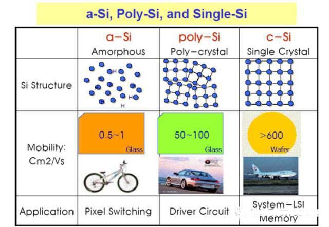
The electron mobility of traditional amorphous silicon material (a-Si) is only 0.5 cm2/V.S, while the electron mobility of low-temperature polysilicon material (LTPS) can reach 50-200 cm2/V.S. Compared with crystalline liquid crystal display (a-Si TFT-LCD), low-temperature polysilicon TFT-LCD has the advantages of higher resolution, fast response speed, high brightness (high aperture ratio), etc. At the same time, the peripheral driving circuit can be made on the glass at the same time. On the substrate, the goal of integrating the system on glass (SOG) can be achieved, so it can save space and cost. In addition, LTPS technology is the technology platform for the development of active organic electroluminescence (AM-OLED), so the development of LTPS technology is subject to broad attention.
2. The difference between amorphous silicon (a-Si) and low temperature polysilicon (LTPS)
In general, the process temperature of low-temperature polysilicon should be lower than 600°C, especially for the requirement of "laser anneal" (laser anneal), a manufacturing process that distinguishes LTPS from a-Si manufacturing. Compared with a-Si, the electron movement speed of LTPS is 100 times faster than that of a-Si. This feature can explain two problems: first, each LTPS PANEL reacts faster than a-Si PANEL; second, the appearance of LTPS PANEL The size is smaller than a-Si PANEL. The following are the significant advantages that LTPS holds over a-Si:
3. The panel system design is simpler;
4. The stability of the panel is stronger;
5. Higher resolution,
Resolution:
Since the p-Si TFT is smaller than conventional a-Si, the resolution can be higher.
The driver IC synthesis of p-Si TFT has two advantages on the glass substrate: first, the number of connectors connected to the glass substrate is reduced, and the manufacturing cost of the module is reduced; second, the stability of the module will be dramatically improved.
3. Preparation method of LTPS thin film
1. Metal Induced Crystallization (MIC): one of the SPC methods. However, compared with traditional SPC, this method can produce polysilicon at a lower temperature (about 500~600°C). This is because the thin layer of metal is coated before crystallization is formed, and the metal component plays an active function of reducing crystallization.
2. Cat-CVD: A method for directly depositing polycrystalline thin films (poly-film) without steam extraction. The deposition temperature may be lower than 300°C. The growth mechanism involves catalytic cracking reaction of SiH4-H2 mixture.
3. Laser anneal: This is the most widely used method at present. Excimer laser is the main power, used to heat and melt a-Si, which contains a low amount of hydrogen and then recrystallized into poly-film.
Low temperature polysilicon technology LTPS (Low Temperature Poly-silicon) was originally a technology developed by Japanese and North American technology companies in order to reduce the energy consumption of the Note-PC display and make the Note-PC appear thinner and lighter. It was around the middle of the 1990s. The technology has begun to move towards the trial stage. OLED, a new generation of organic light-emitting liquid crystal panels derived from LTPS, also entered the practical stage in 1998. Its biggest advantages lie in ultra-thin, light weight, low power consumption, and its own light-emitting characteristics, so it can provide more brilliant colors. And clearer images, and more importantly: the production cost is only 1/3 of ordinary LCD panels.
At present, LTPS-OLED panels have not received the support of most LCD panel companies. In addition to technical patent issues, it is unlikely that the original large-scale LCD factory investment will be abandoned. Production efficiency to compete with LTPS. Therefore, most of the liquid crystal displays on the market still use the traditional liquid crystal, that is, the mainstream amorphous silicon (a-Si). The traditional liquid crystal (a-Si) technology has been very mature after more than 10 years of development. They have considerable experience in the mastery of production technology and panel design technology, and LTPS technology still cannot achieve it in a short period of time. Therefore, although the manufacturing cost of LTPS-OLED panel is much lower in theory, its price still has no advantage at present.
However, as the original intention of the original research and development, the low-temperature polysilicon (LTPS) thin-film transistor can embed the driving element on the glass substrate, greatly reducing and retaining the space of the driver IC, so that the size of the thin-film transistor can be made smaller, and at the same time increase the size of the display. Brightness and reduced power consumption, thereby greatly improving the performance and reliability of liquid crystal, and also reducing the manufacturing cost of the panel, with higher resolution: the TFT active matrix driver provided by LTPS and the driver circuit and TFT can be integrated and manufactured at the same time. In the case of maintaining the advantages of lightness and thinness, the problem of insufficient resolution can be solved (because the transmission speed of electrons in polysilicon is faster and the quality is better), so that the 2.5-inch panel can have a high resolution of 200ppi.
Improve lifespan and reduce energy consumption: As an important indicator for the development of LTPS technology, lowering the temperature of liquid crystals means many things for liquid crystals. Both stability and lifespan have been improved. So far this is only a technically qualitative conclusion. I believe It is also easy for everyone to understand that the working life of the display will be extended at a relatively low temperature; the early Note-PC placed great importance on energy consumption, which is also one of the reasons for developing LTPS. While reducing the operating temperature, the LTPS panel The energy consumption is also greatly reduced. Of course, the energy consumption of LCD monitors is inherently small, which means more to Note-PC than PC monitor.
Size reduction: Although flat-panel displays do not have high requirements for size, the pursuit of lighter and thinner liquid crystal displays has always been a hot spot. Since low-temperature polysilicon (LTPS) thin-film transistors can directly embed driving elements on the glass substrate, Therefore, the shell of the LTPS liquid crystal display can almost only retain the thickness of the liquid crystal panel itself, without reserving the space for the driver IC, and reduce the thickness to the greatest extent.
Low Temperature Poly-silicon (Low Temperature Poly-silicon; LTPS, hereinafter referred to as LTPS) is another new technology in the field of flat panel displays. Next-generation technology following amorphous silicon (Amorphous-Silicon, hereinafter referred to as a-Si).
Polysilicon (polysilicon) is a silicon-based material with a size of about 0.1 to several um, which is composed of many silicon particles. In the semiconductor manufacturing industry, polysilicon is usually treated by LPCVD (Low Pressure Chemical Vapor Deposition), and then annealed at a temperature higher than 900C. This method is called SPC (Solid Phase Crystallization). However, this method is not suitable for the flat panel display manufacturing industry, because the maximum temperature of the glass is only 650°C. Therefore, LTPS technology is especially applied in the manufacture of flat panel displays.
The electron mobility of traditional amorphous silicon material (a-Si) is only 0.5 cm2/V.S, while the electron mobility of low-temperature polysilicon material (LTPS) can reach 50-200 cm2/V.S. Compared with crystalline liquid crystal display (a-Si TFT-LCD), low-temperature polysilicon TFT-LCD has the advantages of higher resolution, fast response speed, high brightness (high aperture ratio), etc. At the same time, the peripheral driving circuit can be made on the glass at the same time. On the substrate, the goal of integrating the system on glass (SOG) can be achieved, so it can save space and cost. In addition, LTPS technology is the technology platform for the development of active organic electroluminescence (AM-OLED), so the development of LTPS technology is subject to broad attention.
2. The difference between amorphous silicon (a-Si) and low temperature polysilicon (LTPS)
In general, the process temperature of low-temperature polysilicon should be lower than 600°C, especially for the requirement of "laser anneal" (laser anneal), a manufacturing process that distinguishes LTPS from a-Si manufacturing. Compared with a-Si, the electron movement speed of LTPS is 100 times faster than that of a-Si. This feature can explain two problems: first, each LTPS PANEL reacts faster than a-Si PANEL; second, the appearance of LTPS PANEL The size is smaller than a-Si PANEL. The following are the significant advantages that LTPS holds over a-Si:
1. It is more feasible to integrate the peripheral circuit of the driver IC on the panel substrate;
3. The panel system design is simpler;
4. The stability of the panel is stronger;
5. Higher resolution,
Resolution:
Since the p-Si TFT is smaller than conventional a-Si, the resolution can be higher.
The driver IC synthesis of p-Si TFT has two advantages on the glass substrate: first, the number of connectors connected to the glass substrate is reduced, and the manufacturing cost of the module is reduced; second, the stability of the module will be dramatically improved.
3. Preparation method of LTPS thin film
1. Metal Induced Crystallization (MIC): one of the SPC methods. However, compared with traditional SPC, this method can produce polysilicon at a lower temperature (about 500~600°C). This is because the thin layer of metal is coated before crystallization is formed, and the metal component plays an active function of reducing crystallization.
2. Cat-CVD: A method for directly depositing polycrystalline thin films (poly-film) without steam extraction. The deposition temperature may be lower than 300°C. The growth mechanism involves catalytic cracking reaction of SiH4-H2 mixture.
3. Laser anneal: This is the most widely used method at present. Excimer laser is the main power, used to heat and melt a-Si, which contains a low amount of hydrogen and then recrystallized into poly-film.
Low temperature polysilicon technology LTPS (Low Temperature Poly-silicon) was originally a technology developed by Japanese and North American technology companies in order to reduce the energy consumption of the Note-PC display and make the Note-PC appear thinner and lighter. It was around the middle of the 1990s. The technology has begun to move towards the trial stage. OLED, a new generation of organic light-emitting liquid crystal panels derived from LTPS, also entered the practical stage in 1998. Its biggest advantages lie in ultra-thin, light weight, low power consumption, and its own light-emitting characteristics, so it can provide more brilliant colors. And clearer images, and more importantly: the production cost is only 1/3 of ordinary LCD panels.
At present, LTPS-OLED panels have not received the support of most LCD panel companies. In addition to technical patent issues, it is unlikely that the original large-scale LCD factory investment will be abandoned. Production efficiency to compete with LTPS. Therefore, most of the liquid crystal displays on the market still use the traditional liquid crystal, that is, the mainstream amorphous silicon (a-Si). The traditional liquid crystal (a-Si) technology has been very mature after more than 10 years of development. They have considerable experience in the mastery of production technology and panel design technology, and LTPS technology still cannot achieve it in a short period of time. Therefore, although the manufacturing cost of LTPS-OLED panel is much lower in theory, its price still has no advantage at present.
However, as the original intention of the original research and development, the low-temperature polysilicon (LTPS) thin-film transistor can embed the driving element on the glass substrate, greatly reducing and retaining the space of the driver IC, so that the size of the thin-film transistor can be made smaller, and at the same time increase the size of the display. Brightness and reduced power consumption, thereby greatly improving the performance and reliability of liquid crystal, and also reducing the manufacturing cost of the panel, with higher resolution: the TFT active matrix driver provided by LTPS and the driver circuit and TFT can be integrated and manufactured at the same time. In the case of maintaining the advantages of lightness and thinness, the problem of insufficient resolution can be solved (because the transmission speed of electrons in polysilicon is faster and the quality is better), so that the 2.5-inch panel can have a high resolution of 200ppi.
Improve lifespan and reduce energy consumption: As an important indicator for the development of LTPS technology, lowering the temperature of liquid crystals means many things for liquid crystals. Both stability and lifespan have been improved. So far this is only a technically qualitative conclusion. I believe It is also easy for everyone to understand that the working life of the display will be extended at a relatively low temperature; the early Note-PC placed great importance on energy consumption, which is also one of the reasons for developing LTPS. While reducing the operating temperature, the LTPS panel The energy consumption is also greatly reduced. Of course, the energy consumption of LCD monitors is inherently small, which means more to Note-PC than PC monitor.
Size reduction: Although flat-panel displays do not have high requirements for size, the pursuit of lighter and thinner liquid crystal displays has always been a hot spot. Since low-temperature polysilicon (LTPS) thin-film transistors can directly embed driving elements on the glass substrate, Therefore, the shell of the LTPS liquid crystal display can almost only retain the thickness of the liquid crystal panel itself, without reserving the space for the driver IC, and reduce the thickness to the greatest extent.
Send Inquiry


X
We use cookies to offer you a better browsing experience, analyze site traffic and personalize content. By using this site, you agree to our use of cookies.
Privacy Policy