 English
 Español
 Português
 русский
 Français
 日本語
日本語 Deutsch
 tiếng Việt
 Italiano
 Nederlands
 ภาษาไทย
 Polski
 한국어
한국어 Svenska
 magyar
 Malay
Malay বাংলা ভাষার
 Dansk
Dansk Suomi
Suomi हिन्दी
Why Specify a 3.5-Inch 212x318 TFT LCD for Price-Sensitive Handhelds?
Hardware teams designing budget-conscious handhelds are frequently trapped between two conflicting requirements. Marketing wants a screen large enough to display legible data and touch targets—usually pushing for a 3.5-inch diagonal. Purchasing, meanwhile, mandates a strict bill of materials (BOM) ceiling that rules out high-end microprocessors and external memory.
Engineers often default to standard HVGA (320x480) or QVGA (240x320) panels out of habit. That choice triggers a cascade of hidden costs. Higher pixel counts demand larger frame buffers, forcing the design off a cheap microcontroller and onto a pricier MPU with external SDRAM. The resulting board is larger, more complex to route, and significantly more expensive to manufacture.
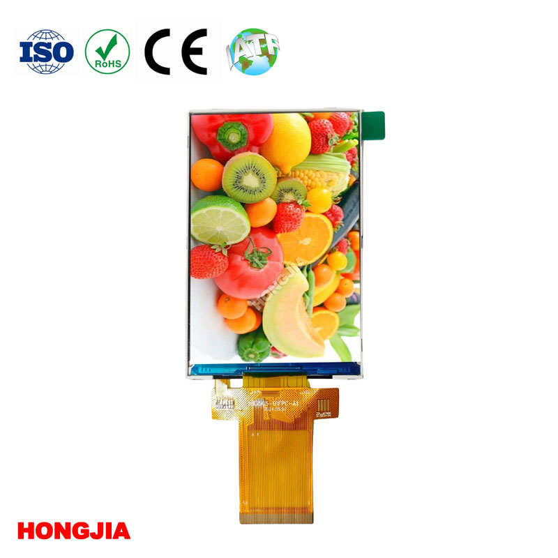
Stepping down to a 3.5 inch TFT LCD 212x318 resolves this conflict. By combining the physical dimensions users expect with a deliberately restricted pixel density, this display format keeps frame buffer requirements small enough to fit inside the internal SRAM of standard, low-cost microcontrollers.
Reducing BOM Costs Through Optimized Resolution and Memory Footprint
The core advantage of the 212x318 resolution is mathematical. Display memory requirements scale linearly with total pixels. When you drive a standard 320x480 display at 16-bit color depth (RGB565), you need roughly 300 kilobytes of RAM just to hold a single frame. Double buffering pushes that to 600 kilobytes. Most entry-level and mid-range Cortex-M microcontrollers lack that kind of onboard capacity.
A 212x318 display drops the single-frame memory requirement to roughly 134 kilobytes. That footprint fits comfortably inside the internal SRAM of economical MCUs. You eliminate the need for an external RAM chip entirely.
Removing external memory from your schematic yields compound benefits:
- Direct component savings: You cut the cost of the RAM chip itself.
- Reduced layer count: Routing high-speed memory interfaces often forces designers from a 4-layer PCB to a 6-layer board. Staying internal keeps manufacturing cheap.
- Lower power consumption: Internal SRAM access draws a fraction of the power required to drive external traces, extending the runtime of handheld devices.
This is what defines a true low cost 3.5 inch LCD module. The savings extend far beyond the price of the glass itself, fundamentally lowering the cost architecture of the entire mainboard.
Interface Flexibility: Routing SPI, MCU, or RGB Connections to the ST7789 Driver
Budget projects rarely have the luxury of dedicating dozens of GPIO pins to a display. The HJ3505-01 utilizes the widely supported ST7789 driver IC, offering hardware teams the choice between SPI, MCU (8080 parallel), and RGB interfaces. Your choice here dictates both your pin budget and your maximum refresh rate.
For applications displaying mostly static data—like digital thermometers, industrial multimeters, or simple smart home controls—SPI is the logical choice. An ST7789 3.5 inch TFT LCD wired for 4-line SPI requires only a handful of pins. You sacrifice the bandwidth needed for fluid 60fps video, but you free up critical routing channels for sensors and communication modules.
When the UI requires faster updates or simple animations, the MCU (8080) interface provides a middle ground. It reads and writes directly to the ST7789's internal GRAM, moving data fast enough for responsive menus without demanding the continuous clocking of a raw RGB connection.
If your application demands smooth, continuous motion and your processor includes an integrated display controller, you can bypass the internal GRAM and drive the panel via the RGB interface. Be aware of the trade-off: RGB requires continuous data streaming, which consumes processor cycles and up to 24 dedicated GPIO pins, potentially offsetting the cost benefits if it forces you into a larger MCU package.
Deploying High-Brightness Portrait Screens in Smart Home Panels and Handheld Instruments
Handheld diagnostics and smart wall panels share a common physical constraint: they are primarily used in a vertical orientation. Specifying a native 3.5 inch vertical TFT display prevents the software overhead of rotating the user interface in memory—a process that burns precious CPU cycles on low-end hardware.
Visibility dictates usability in these environments. A transmissive 3.5 inch LCD panel relies entirely on its backlight to punch through ambient light. In clinical settings with harsh overhead fluorescents, or smart home panels hit by direct morning sunlight, standard 250-nit displays wash out. A high brightness 3.5 inch vertical screen (typically rated at 500 nits or above) maintains contrast and legibility under glare.
However, high brightness comes with a thermal and power penalty. Driving LEDs at maximum current continuously will drain a small LiPo battery fast and generate localized heat that can skew nearby temperature sensors inside an environmental control panel. Engineers must manage the backlight actively rather than leaving it pinned at 100 percent.
Extending Battery Life with AI-Driven Dynamic Backlight Dimming in 2026
As we look toward the next generation of embedded designs, power management is shifting from simple ambient light sensors to predictive, edge-AI models. By 2026, low-power microcontrollers will increasingly run lightweight machine learning algorithms capable of dynamic backlight dimming.
Instead of merely dimming the screen in dark rooms, these models analyze the actual content being rendered. If a medical instrument displays a high-contrast numeric readout on a dark background, the algorithm can simultaneously boost pixel gamma and drop the physical backlight voltage. This content-adaptive approach preserves perceived brightness while slashing power consumption by up to 30 percent, keeping transmissive panels viable for tightly constrained battery-operated devices.
Validating HONGJIA Manufacturing Standards for US-Based Embedded Projects
Sourcing low-cost displays for US-bound industrial or medical equipment carries inherent compliance risks. A cheap panel is useless if the flexible printed circuit (FPC) tears during assembly or fails under thermal cycling in the field.
HONGJIA mitigates these risks through controlled manufacturing environments rather than manual assembly. The company relies on automated COG and FOG bonding equipment. Chip-on-Glass (COG) and Film-on-Glass (FOG) bonding require precise temperature and pressure profiles to ensure the anisotropic conductive film (ACF) cures perfectly. HONGJIA executes this entirely within cleanrooms, preventing microscopic dust ingress that causes dead columns or intermittent touch failures months after deployment.
For engineering teams working on regulated hardware, facility certifications are non-negotiable. HONGJIA operates under ISO 9001 (Quality) and ISO 14001 (Environmental), alongside ISO 45001. Crucially for diagnostic and patient-monitoring devices, the facility holds ISO 13485 certification, demonstrating the traceability and quality management required for medical device supply chains.
If you are engineering a device where BOM cost is critical but field failure is unacceptable, reviewing the exact specifications of the glass, the FPC length, and the backlight configuration is your next step. Evaluate the HJ3505-01 212x318 portrait display module to see how an optimized resolution can streamline your hardware architecture.
Send Inquiry


X
We use cookies to offer you a better browsing experience, analyze site traffic and personalize content. By using this site, you agree to our use of cookies.
Privacy Policy